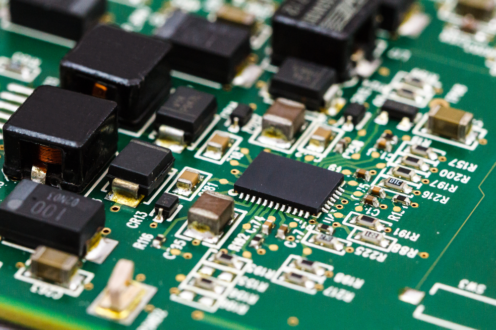
Application-Specific Integrated Circuits (ASICs)
Found in almost any electronic device and designed for a wide range of applications, ASICs (application-specific integrated circuits) have become an integral part in many product technologies, particularly custom-made ones.
Unlike a programmable logic device or standard logic IC, an ASIC is designed to do one specific thing and it does this one thing very well, enabling it to perform faster. This type of IC can be made smaller and also consumes less electricity.
But it is more expensive to produce and is considered proprietary technology since it is custom-made for the company that needs it.
There are three categories of ASICs:
- Full custom ASICs – Custom-designed from scratch for a specific application.
- Semi-custom ASICs – Partly customized to perform different functions and allow some modifications.
- Platform ASICs – Uses predefined platform slices made from a defined set of methodologies.
How ASICs are Designed and Fabricated
There are several essential questions that require answering prior to beginning the development of an ASIC:
- What are the system requirements to be achieved?
- What are the chip specifications and constraints to be defined?
- What are the necessary ASIC required specifications?
Furthermore, there are specific preliminary designs processes that need to be followed in order to complete the design. These include:
- Full understanding and knowledge of how to use Electronic design automation (EDA) tools. EDA are software tools for designing electronic systems such as integrated circuits and printed circuit boards.
- The production of a Block diagram
- The packaging of the ASIC according to the required packaging requirements
- The development of the testing procedures and the test equipment needed for the testing of the product
- The development of a scheduled timeline for completion
- The choice of die size
- The fabrication process (in house or fabless)
Here is the ASIC flow chart from Linear Microsystems Inc. (LMI), located in Irvine, CA. and an expert in ASIC design and production. Listed below are the intricate steps that LMI follows to successfully complete the ASIC:
- Specification and Architecture Development
- Key specifications, pinout, major block definition, the package definition
- Conceptual Cell Design
- Preliminary design and simulations of major functional blocks over nominal conditions
- Verify Key Specs, Process Choice and Die Size
- Preliminary Cell Design
- Detailed design and simulation of major functional blocks over PVT (process, supply, temperature)
- Final Cell Design
- Detailed design of all functional blocks
- Top Level Design
- Top level simulations; worst case simulations
- Physical Design
- Custom cell layout and verification, automatic placement and routing, verification, parasitic extraction, and post-layout simulation
- Prototype Evaluation
- Evaluation of small quantity of samples
- Re-spin if necessary
- Qualification
- Fabrication of low quantity production lot; tested using in-house ATE system
- Qualification Testing
A few more details:
Materials Used
ASICs are made from a wafer which is produced using the Czochralski process where extremely pure silicon is grown into mono-crystalline cylindrical ingots. The ingots or boules are grown up to 300 mm in diameter. It is then sliced into about 0.75 mm thick wafers and then polished until a very flat and regular surface is achieved.
Front-End/RTL Design
Register Transfer Level (RTL) design is a method by which one can transfer data from one register to another.
For digital ASICs or for digital blocks within a mixed-signal chip, this phase is basically the detailed logic implementation of the entire ASIC based an on the functional requirements of the chip. It is at this time that the detailed system specifications are converted into Verilog language and that a verification process is performed to ensure that the RTL design is done according to the given specifications.
Back-End Processing
This is where the chip is physically laid out and implemented, also known as the “floorplanning” process. The software is used to place the RTL design on the chip footprint.
The general workflow of the back-end process involves:
- Floorplanning – Physical implementation of the chip.
- Placement of individual gates – Gates involved in the same computations is set physically close together.
- A building of clock trees – Ensure that each clock reaches each gate at the right time through a well-designed clock distribution network.
- Routing – Connections between gates are auto-routed using software since the manual routing of thousands or millions of connections would take a long time to complete.
- Optimization – Uses design rule checking (DRC) to ensure that the design is physically manufacturable.
- Static timing analysis – Layout versus schematic checks to ensure that the desired circuitry is achieved with the physical geometries.
Once frontend and backend processing are complete, “tape out” follows. In this stage, the final design of the chip is prepped for production
Manufacturing
Different techniques are used to produce ASICs. These include a combination of acid baths, photolithography, furnace annealing, ion implantation, and metallic sputter deposition.
Once manufactured, the wafer is then tested for fabrication errors. Scan testing is used to check failures for each individual gate.
Packaging
Custom packaging is usually designed for the working die, with consideration to thermal regulation, cost, signal integrity, and design reliability. Once a die is placed in its custom packaging, it is re-tested. The die is then sealed.
Another packaging technology is the chip scale package which, as the name suggests, is designed at nearly the same size as the die.
ASIC design is highly complex and requires significant technical expertise. Linear Microsystems has highly qualified experts in the design, development, and production of high-performance mixed-signal ASICs and is partnered with a world-class engineering team and associated with some of the world’s leading foundry and packaging vendors.
For any questions you might have regarding ASICs please call Peninsula Technical Sales where we have experts to help you answer any of your questions. You can reach us by calling 650-965-3636, by e-mailing us at sales@pentech.com or continue visiting our website.
Peninsula Technical Sales represents electronic equipment manufacturers and is proud to offer our services online and to the following cities and their surrounding areas: San Francisco, Santa Clara, San Jose, Fremont, Sacramento, Milpitas, and Santa Rosa.